Curated with aloha by
Ted Mooney, P.E. RET

The authoritative public forum
for Metal Finishing 1989-2025

-----
Non-wetting defect on NiPdAu plating
We are encountering "Non-wetting" defects for all IC's Having Nickel Palladium Gold (Lead Free) plating. The solder paste the we are using was still SnPb (WATER SOLUBLE). Crack plating on the bend area of the IC leads was observed leading to exposed copper. We just want to know the criteria of the crack plating and its effect to solderability.
Joel MacalindongIntegrated Microelectronics - Sta Rosa, Laguna, Philippines
2005
The only thing to prevent cracking on plated portion after bending is to do forming first before plating. It is possible but need to do a lot of modification on the process. Try to do baking before forming at 150 °C at 1 hour. We tried it and it helps a bit compare than no baking.
Irvy Cane Boltron- Singapore
2005
September 28, 2011
Dear All,
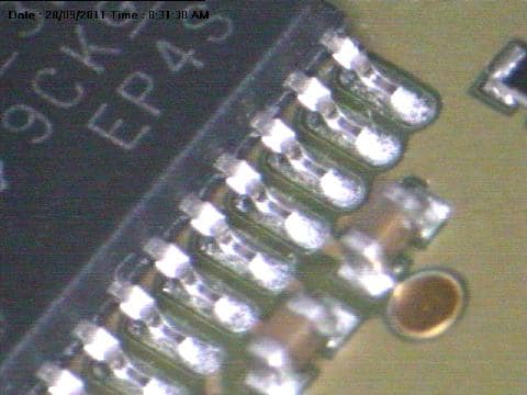
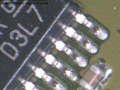
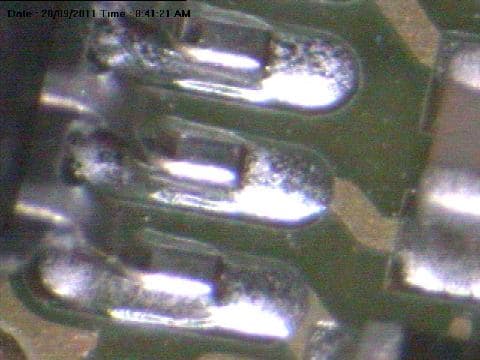
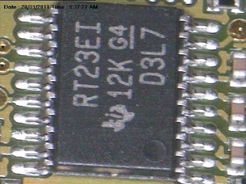
I'm from Engineering group facing intermittent soldering on TSSOP lead where visual inspection shown incomplete wetting or due to exposed copper at lead cutting edge. Would like to understand the process flow of Semiconductor IC where after plating process, do they need to perform cleaning or not. From our knowledge, there is cleaning process to removed any chemical/oil to avoid solderability issue to the component lead. Will this may lead to defect shown below.


Engineer - Penang, Malaysia
Q, A, or Comment on THIS thread -or- Start a NEW Thread